Why Does Impedance Drift from Your Design Target?
You run your differential pair through a SI simulator, dial in 100Ω, and sign off the stackup. The boards come back from the fab. You probe the TDR coupon and read 93Ω — or 108Ω. This gap between design intent and manufactured reality is one of the most common headaches in high-speed PCB production, and it never has a single cause.
Differential impedance deviation is the cumulative result of four independent error chains: material properties, lamination, etching, and copper thickness. This article breaks down each one from the manufacturer's perspective — with real numbers — so you can understand where the tolerance budget is being spent, and what levers actually move the needle.
Section 1: What Actually Controls Differential Impedance
The differential impedance Zdiff of a coupled transmission line is governed by five physical parameters:
- W — trace width
- S — spacing between the differential pair
- H — dielectric thickness from signal layer to reference plane
- T — copper thickness
- Dk — dielectric constant of the substrate material
None of these are exact. Every one carries a manufacturing tolerance, and those tolerances stack. Based on statistical analysis using ADS CILD with a 10% variation applied to each parameter independently against a 100Ω differential target, the impact ranking looks like this:
| Parameter | 10% variation → impedance swing | Risk level |
|---|---|---|
| H (dielectric thickness) | ±10Ω | HIGHEST |
| Dk (dielectric constant) | ±6.5Ω | HIGH |
| W (trace width) | ±5Ω | MEDIUM |
| S (pair spacing) | ±3.5Ω | LOW-MED |
| T (copper thickness) | ±1.5Ω | LOW |
The takeaway is counterintuitive for many designers: dielectric thickness H is the single biggest variable, yet most impedance discussions revolve around trace width. Spending hours optimising trace width compensation while ignoring lamination process control is working the wrong end of the problem.
Section 2: Material Selection — The Hidden Dk Problem
FR4 is quoted with a nominal Dk of around 4.2, but that number carries three traps that aren't obvious from a datasheet.
Trap 1: Frequency dependence. FR4's Dk at 1 GHz is approximately 4.2. At 10 GHz it drops to roughly 3.8. High-speed serial buses — PCIe 5.0, USB4, 10GbE — operate in the multi-GHz range. If your stackup calculator is using the low-frequency Dk, the calculated trace width will produce impedance that runs high on the actual board. The error is systematic and consistent, which at least makes it correctable — but only if you know to look for it.
Trap 2: Lot-to-lot variation. Two rolls of nominally identical FR4 from the same manufacturer can have Dk values that differ by 0.2–0.3. For a 100Ω differential target, that Dk swing translates to roughly 3–4Ω of impedance variation — before any other process variables are applied.
Trap 3: Resin content non-uniformity. During lamination, prepreg resin flows differently in the centre of the panel versus the edges. The resulting Dk gradient across a large panel is one of the primary reasons impedance repeatability degrades on boards larger than 300 × 400 mm.
What good fabs actually do: Require each incoming material lot to be accompanied by a measured Dk report taken at the target operating frequency. Use that measured value — not the datasheet nominal — as the input to stackup calculations. For RF or high-speed applications, Rogers, Isola, or PTFE materials with Dk stability within ±0.05 are the correct choice; FR4 is not a high-frequency material.
Section 3: Stackup and Lamination — Controlling H is the Core Problem
The dielectric thickness H comes from two contributors: core laminate thickness plus the post-lamination thickness of the prepreg. Core thickness is relatively stable, typically within ±5%. Prepreg post-press thickness is where the real variation lives.
Two lamination parameters drive the outcome: resin flow volume and press pressure uniformity.
A standard 2116 prepreg has a nominal thickness of 0.11 mm. After lamination, the actual pressed thickness may be only 0.095 mm — a 13% reduction. If your stackup calculation uses the nominal pre-press spec rather than the measured post-press value, you are starting with a systematic error of roughly 7Ω before the board is etched.
Pressure uniformity is the large-panel problem. In a press cycle, pressure is transmitted through cushion pads. On panels larger than 300 × 400 mm, the cushion compresses approximately 15–20% more at the edges than at the centre. The result: centre-panel resin fill is insufficient, the dielectric is thicker in the centre, and impedance runs lower there than at the edges. The measured impedance delta between centre and edge can reach 6–8Ω on large panels without specific mitigation.
Mitigation requires either pressure-equalising tooling inserts during lamination, or a zone-by-zone press parameter programme that compensates for the known pressure gradient.
Rule: Stackup impedance calculations must use the fab's measured post-press dielectric thickness, not the prepreg datasheet value. If a fab cannot supply this data, their impedance control is guesswork.
Section 4: Etching and Trace Width — How Compensation Works
Trace width is the third-largest impedance variable and also the most actionable one from a process engineering standpoint. The fundamental issue is that wet etching is not directional: the etchant attacks copper from the top and from the sides simultaneously. This lateral attack — called undercut — means the finished copper trace has a trapezoidal cross-section, not the rectangular profile implied by the Gerber file.
Typical undercut values: 0.5–1.0 mil (12–25 μm) per side on outer layers, reducible to below 0.3 mil with precision etching chemistry and controlled dwell time. The effective trace width after etching is narrower than the artwork width by 2× the undercut value.
To compensate, the engineering department widens the trace in the production artwork — positive compensation — so that the post-etch width lands on the target. The compensation amount equals 2× the measured undercut for that layer and etch chemistry.
Three details that are frequently overlooked:
Isolated vs. dense traces etch differently. In dense trace regions, etchant exchange is constrained, undercut is reduced. Isolated impedance-controlled traces surrounded by open copper have full etchant access and undercut more aggressively. A single flat compensation value applied across the board introduces a systematic error between dense and sparse regions. Proper process engineering sets different compensation values by zone.
Differential pair spacing S is also affected. If both traces in a pair undercut by 0.5 mil per side, the gap between them grows by 1.0 mil. On a 100Ω differential line, a 1 mil gap increase adds approximately 2–3Ω. This is an independent error from the width effect and must be accounted for separately in the compensation calculation.
No repairs on impedance traces. Any jumper or conductive touch-up on an impedance-controlled trace changes the local cross-section discontinuously. The repair site will show as a distinct spike on a TDR trace. IPC Class 3 boards prohibit conductor repairs on controlled-impedance features; this should be a rejection criterion, not a judgment call.
Section 5: Copper Thickness Uniformity — The Indirect Effects
Copper thickness T has the smallest direct impedance impact of the five parameters (±1.5Ω for a 10% variation). But non-uniform copper thickness creates two indirect failure modes that amplify the other error sources.
Indirect effect 1: Non-uniform etch rate across the panel. Thicker copper takes longer to etch through. If the etch time is set for the thinner areas, the thicker areas are underetched and traces are too wide; if set for the thicker areas, the thinner areas are over-etched and traces are too narrow. On a panel with a ±10% copper thickness gradient, the resulting trace width variation can be 0.5–1.5 mil, representing 3–5Ω of impedance spread — turning a T variable into a W variable.
Indirect effect 2: Via copper uniformity in high aspect ratio boards. Plated-through holes in boards thicker than 2.4 mm with via diameters below 0.3 mm show significant copper thickness variation from top to bottom of the barrel. This affects via impedance, which is a separate but related concern for high-speed differential signals passing through layer transitions.
Copper thickness uniformity is controlled through: thieving copper patterns in sparse areas to balance current density during electroplating, adjusting anode-to-board geometry in the plating tank, and pre-treatment to improve surface receptivity uniformity before copper deposition.
Section 6: Same-Layer vs. Cross-Layer Differential Routing
This is a design decision with significant manufacturing consequences. Differential pairs can be routed in two configurations:
Side-by-side (same layer): Both traces run on the same signal layer, separated by the gap S. The spacing accuracy is determined by etch precision, which can hold ±0.5 mil under normal conditions. This is the preferred configuration.
Over-under (adjacent layers): One trace runs on L2, the other on L3. The "spacing" between them is now the inter-layer dielectric thickness — which is set by the lamination process, not by etch precision. Lamination thickness tolerance is substantially worse than etch tolerance, and localised resin flow variation means the inter-layer distance is not constant across the panel.
Empirically, over-under differential pairs show 30–50% worse impedance uniformity than same-layer pairs built to the same nominal specification. Unless board routing geometry makes same-layer differential physically impossible, cross-layer differential routing should be avoided for controlled-impedance high-speed signals.
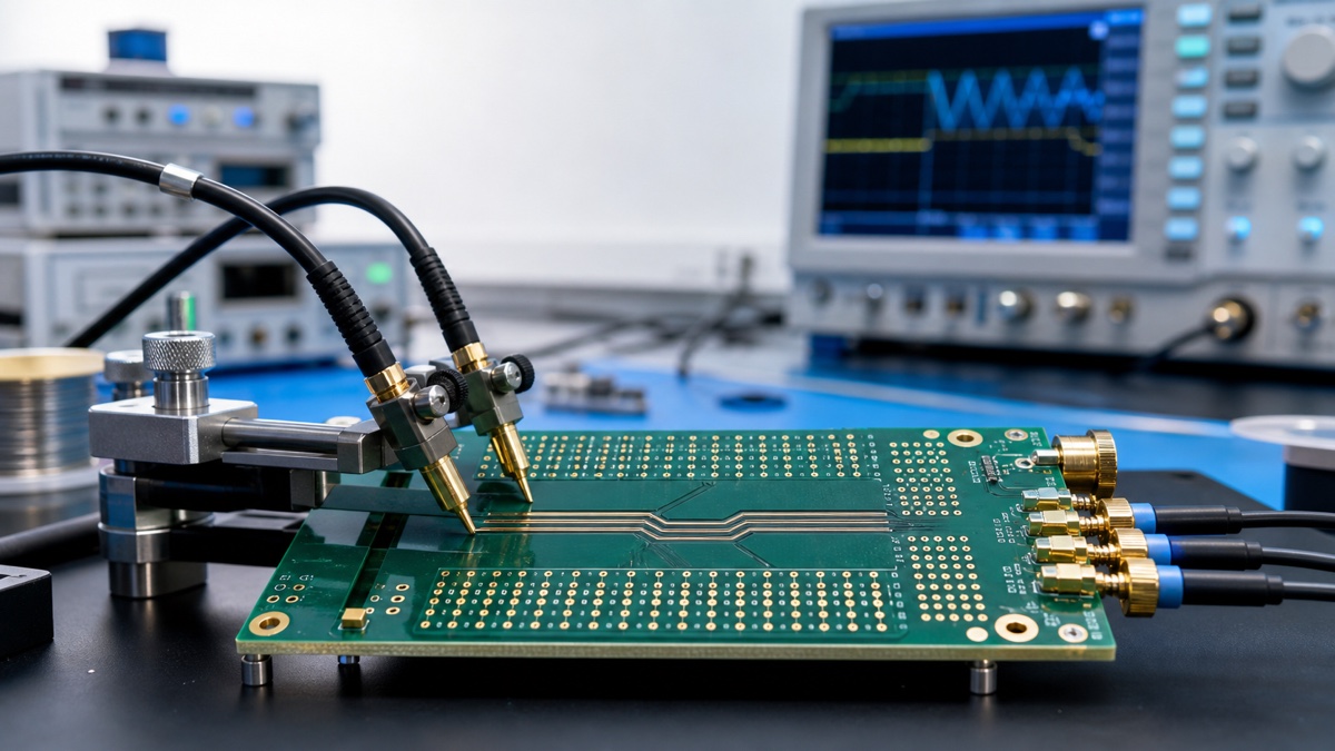
Section 7: TDR Verification — Reading the Test Report
Time Domain Reflectometry (TDR) is the industry-standard method for impedance verification, governed by IPC-TM-650 2.5.5.7a. The instrument injects a fast rising-edge step signal into the trace under test. At any point where impedance is discontinuous, a reflection is generated and travels back toward the source. By timing and measuring that reflection, the instrument reconstructs the impedance profile of the trace as a function of position.
Rise time determines resolution. A TDR system with a 28 ps rise time can resolve impedance discontinuities separated by approximately 2 mm. A 300 ps system is limited to about 20 mm resolution. For via-level impedance analysis on high-speed backplanes, only high-bandwidth TDR is adequate. Entry-level instruments used for production screening may pass a board that a high-resolution instrument would flag.
Testing is done on coupons, not on the circuit. A TDR coupon is a dedicated test structure laminated in the panel edge alongside the production boards. It shares the same lamination cycle, the same copper plating bath, and the same etch run as the main board. Its trace geometry is designed specifically for TDR probing — a long controlled-impedance run with accessible probe pads. Reading the coupon gives you the process result; it does not tell you about localised anomalies in the main board.
What the waveform tells you:
- A flat line at the target impedance — the ideal result
- A sustained upward shift — trace width is consistently narrow (over-etch) or dielectric is thick
- A sustained downward shift — trace width is too wide (under-etch) or dielectric is thin
- A spike at a single location — a local discontinuity: a repair, a width transition, a via, or a pad stub
First-article failure response. If the first-article TDR reads 107Ω against a 100Ω target, the next step is root cause analysis, not re-spin guesswork. Measure the actual etched trace width. Measure the post-press dielectric thickness. If the trace is narrow, increase the etch compensation and re-run. If the dielectric is thinner than the stackup calculation assumed, revise the calculation and adjust the trace width target. Iterate until the coupon reads within tolerance, then release to production quantity.
Section 8: Production Statistical Control
A passing first-article coupon confirms the process was correct at the start of the run. It does not guarantee the run stays in control. Mature fabs apply Statistical Process Control (SPC) to impedance data:
- Sample 3–5% of coupons per lot for TDR measurement
- Track the mean and standard deviation of measured impedance over time
- Set control limits at ±3Ω from nominal; if the mean drifts past this threshold, trigger a process review before continuing production
- If standard deviation begins trending upward across consecutive lots, investigate material lot change, etchant bath chemistry drift, or lamination parameter creep
For automotive and RF applications, an additional environmental qualification is typically required: temperature cycling from -40°C to +125°C for 100 cycles, with post-cycle impedance change ≤ ±2% (automotive Class 2) or ≤ ±1.5% (RF/communications). This test verifies that the dielectric material and copper adhesion remain stable over the thermal range of the end application — a concern that room-temperature TDR alone cannot address.
Summary: The Error Budget Framework
Controlling differential impedance to within ±10% of the design target — or tighter, for high-reliability applications — requires treating it as a system problem, not a single-step specification. Every process stage contributes to the total error budget:
| Process stage | Primary control method | Impedance impact |
|---|---|---|
| Material | Incoming Dk measured per lot at target frequency | ±6.5Ω |
| Lamination / stackup | Use post-press measured H; pressure equalisation tooling for large panels | ±10Ω |
| Etch compensation | Zone-differentiated compensation; separate isolated vs. dense regions | ±5Ω |
| Copper thickness | Thieving copper design; plating current distribution control | ±1.5Ω |
| Routing strategy | Same-layer differential pairs wherever possible | Uniformity +30–50% |
| TDR verification | High-bandwidth instrument; first-article closed-loop; SPC on production | Detect and correct deviations |
When you understand this chain, the conversation with your manufacturer changes. Instead of specifying "100Ω ±10%" and hoping for the best, you can ask specific questions: What is the measured post-press dielectric thickness for this stackup? What etch compensation values are you applying for this layer? Can you supply per-lot Dk data for the prepreg? Those are the questions that separate a controlled impedance process from a nominal impedance guess.
This article covers FR4 multi-layer microstrip and stripline configurations. Rogers, PTFE, and other low-loss high-frequency materials follow the same process logic but with different absolute values and tighter inherent tolerances — we will cover those in a separate article.